




Automated Optical Inspection (AOI) in PCB Manufacturing
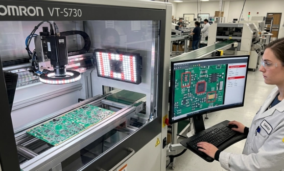

Automated Optical Inspection (AOI) is a machine vision-based technology used to inspect surface-level defects in PCB assemblies using high-resolution cameras and image processing algorithms.
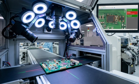
It is widely used in SMT production lines for real-time quality control.
AOI Working Principle
AOI systems operate by:
- Capturing PCB image
- Comparing with reference “golden board”
- Detecting deviations
- Flagging defects automatically
What Does AOI Inspect?
AOI systems are engineered to capture a wide range of defects and anomalies throughout the electronics manufacturing process. By leveraging advanced imaging algorithms and analytical techniques, AOI ensures full-spectrum quality control from bare boards to final assembly.
1. Component Defects
Component-related issues are critical to a product's functionality and long-term reliability. AOI systems focus on identifying:
- Missing Components: Detects parts that were never placed, fell off during reflow, or were accidentally removed during handling.
- Wrong Components: Identifies incorrect values, mismatched specifications, or polarity reversals.
- Placement Errors: Catches incorrect package sizes, skewed orientations, or component type mismatches.
2. Solder Joint Abnormalities
The quality of a solder joint determines both electrical connectivity and mechanical stability. AOI excels at detecting:
- Cold Solder Joints: Caused by insufficient heat during reflow, resulting in poor wetting.
- Solder Bridging: Unwanted connections between adjacent pads that lead to short circuits.
- Insufficient Solder: Inadequate solder volume that fails to create a reliable or permanent connection.
3. Solder Paste Issues
Solder paste printing defects are the root cause of 60-70% of assembly failures. Detecting these before component placement prevents costly rework:
| Defect Type | Description | Potential Impact |
| Insufficient Volume | Solder amount is below specified requirements | Weak joints and poor electrical contact |
| Excessive Solder | Solder volume exceeds allowed specifications | High risk of bridging and short circuits |
| Misalignment | Paste is not centered on the pads | Component shifting and poor connectivity |
| Shape Distortion | Irregular or uneven paste deposits | Unpredictable behavior during reflow |
4. Hidden Solder Issues
Advanced 3D AOI systems go beyond the limitations of traditional 2D methods. By analyzing height and volume, 3D AOI can identify hidden defects in complex, high-density packages (such as BGA or QFN), inspecting critical factors like heel fillets and co-planarity.
5. Bare PCB Defects
Prior to assembly, AOI can be used to inspect bare boards for fabrication defects that might compromise the final product, such as trace shorts, opens, copper splashes, or solder mask violations.
Here is the professional English version of the Core Advantages of AOI, written with a focus on operational excellence and high-tech manufacturing standards.
The Strategic Value of AOI: Empowering Manufacturing Excellence
The integration of AOI (Automated Optical Inspection) technology brings transformative benefits to electronics manufacturing. Beyond simple defect detection, it serves as a catalyst for operational efficiency, cost optimization, and unparalleled quality assurance.
1. Exceptional Efficiency
AOI systems can inspect hundreds of components per minute, significantly outpacing manual inspection methods.
- Speed Advantage: Operates up to 50 times faster than human visual inspection.
- 24/7 Productivity: Capable of continuous, around-the-clock operation without performance degradation.
- Parallel Processing: Simultaneously analyzes multiple inspection points to maintain high throughput without compromising quality.
2. Superior Accuracy
Utilizing high-resolution imaging and advanced algorithms, AOI systems detect microscopic flaws—down to 25 microns—that are invisible to the naked eye.
- Precision Performance: Achieves an inspection accuracy rate exceeding 99.5%.
- Unwavering Standards: Eliminates subjectivity and maintains consistent performance regardless of lighting or environment.
- Micro-Defect Detection: Captures subtle anomalies in ultra-fine pitch components and high-density layouts.
3. Enhanced Traceability
In a data-driven manufacturing environment, AOI provides a complete digital footprint of the quality control process.
- Digital Records: Generates comprehensive inspection logs and images for every board, ensuring 100% traceability.
- SPC Integration: Seamlessly integrates with Statistical Process Control (SPC) to track defect trends and prevent systemic issues.
- Continuous Improvement: Enables data-backed decision-making through historical trend analysis and process optimization.
4. Significant Cost Reduction
By catching defects early in the production cycle, AOI prevents the heavy financial burden of late-stage failures.
- Minimized Rework: Intercepting errors at the printing or placement stage reduces scrap and expensive post-reflow repairs.
- Labor Optimization: Automation reduces the dependency on large inspection teams, lowering long-term operational overhead.
- Reduced Warranty Claims: Enhances field reliability, significantly lowering the costs associated with returns and warranty service.
5. Unmatched Consistency & Reliability
Unlike human inspectors who are prone to fatigue, AOI maintains a constant level of performance throughout the entire production run.
- 99.8% Repeatability: Ensures identical inspection criteria are applied across every batch.
- Zero Fatigue Factor: Maintains peak performance levels from the first hour of production to the last.
- Standardized Control: Guarantees that every product meets a uniform, rigorous quality benchmark regardless of production volume.
AOI System Types
The evolution of AOI technology has branched into two primary methodologies. Understanding the distinct advantages of each allows you to find the perfect balance between inspection depth, production speed, and manufacturing costs.
1. 2D AOI: The High-Efficiency Industry Standard
2D AOI systems utilize top-down planar imaging to capture high-resolution views of the PCB surface. For many standard assembly requirements, it remains the most cost-effective and reliable solution.
- Core Capabilities:
- Placement Verification: Precise detection of missing components, polarity reversals, and orientation errors.
- Surface Analysis: Reliable identification of visible surface defects and solder paste coverage.
- Strategic Advantages:
- Cost-Effectiveness: Lower initial investment (CAPEX) compared to 3D systems.
- Exceptional Speed: Faster processing cycles that seamlessly match high-speed production lines.
- Rapid Deployment: Simplified programming and setup, ideal for high-mix, low-volume (HMLV) environments.
2. 3D AOI: The Pinnacle of Precision and Depth
3D AOI employs advanced laser scanning or structured light projection to incorporate the "Height" dimension. It is the gold standard for inspecting complex packages and high-reliability electronics.
- Advanced Technical Features:
- Volumetric Measurement: Precise calculation of solder joint height, volume, and component co-planarity.
- Complex Package Excellence: Superior performance in inspecting BGA, QFN, and other bottom-terminated components.
- Hidden Defect Detection: Identifies "lifted leads" or "Head-in-Pillow" (HoP) effects that are often invisible to 2D sensors.
- Operational Superiority:
- Reduced False Positives: Digital height data significantly lowers the false call rate common in 2D shadow-prone layouts.
- Comprehensive Coverage: Provides 100% inspection surface area, meeting the stringent standards of the automotive and aerospace industries.
- Future-Proofing: An essential investment for modern, ultra-miniaturized designs.
- AOI Limitations
- Cannot detect hidden solder joints
- Sensitive to lighting conditions
- May generate false positives
AOI vs AXI
| Feature | AOI | AXI |
| Visibility | Surface | Internal |
| Speed | Fast | Slower |
| Defect type | External | Hidden |
AOI in SMT Process Flow
- Solder paste inspection (SPI)
- Pre-reflow AOI
- Post-reflow AOI
- Final PCB AOI
As the electronics manufacturing landscape undergoes rapid transformation, YSX remains at the vanguard of AOI (Automated Optical Inspection) innovation and implementation.
Our holistic approach to quality assurance—integrating cutting-edge 3D AOI systems with AI-driven detection algorithms—guarantees that every product fulfills the most stringent global quality standards. By harmonizing precision with efficiency, YSX empowers your innovations with uncompromising reliability while maintaining a competitive edge in manufacturing costs.
Ready for Production? Kickstart Your Project Now. info@ysx-tech.com
Unsure About the Design? Consult with Our Lead Engineers Today. contact us
Share on Social:


- PREV: Design Rule Check (DRC)
- NEXT: PCB Layer Stackup