




The Complete Guide to PCB E-Test

Introduction
As PCB designs continue to evolve toward higher density, finer pitch, and faster signal speeds, traditional inspection methods such as visual checks or AOI are no longer sufficient.
Even microscopic defects—such as hairline opens or internal shorts—can lead to catastrophic failures after assembly.
This is why PCB Electrical Testing (E-Test) has become a mandatory step in modern PCB manufacturing, ensuring that every circuit performs exactly as designed.
What Is PCB E-Test?
PCB E-Test (Electrical Test) is a process used to verify that the fabricated PCB matches the original electrical design (netlist).
It checks for:
- Open circuits (missing connections)
- Short circuits (unwanted connections)
- Insulation failures
- Electrical leakage issues
Unlike visual inspection, E-test directly validates the functional electrical integrity of the board.
Why PCB E-Test Is Critical in Modern Manufacturing
1. Increasing PCB Complexity
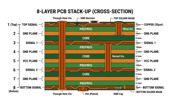
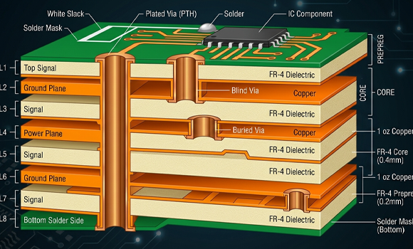
Modern PCBs include:
- HDI structures
- Microvias and stacked vias
- Fine-pitch BGAs
- High-speed differential pairs
These features significantly increase the risk of hidden electrical defects.
2. Cost of Failure Escalation
| Stage | Cost Impact |
|---|---|
| Bare PCB stage | Low |
| After assembly | Medium |
| After shipment | Extremely high |
👉 Detecting defects early can reduce total cost by 10x–100x.
3. Reliability Requirements
Industries such as:
- Automotive
- Medical
- Aerospace
require near-zero defect tolerance, making E-test indispensable.
Core PCB E-Test Methods
Flying Probe Testing
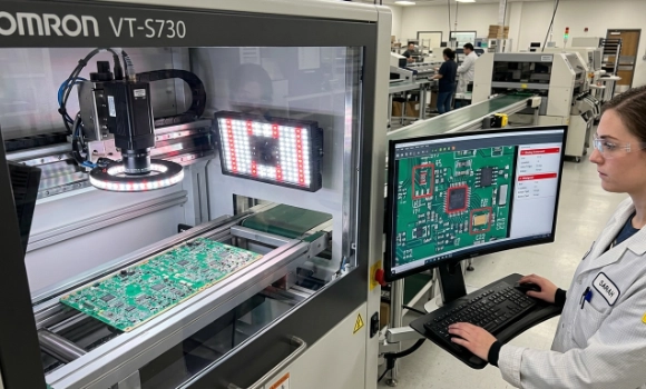
Flying probe testing uses movable probes controlled by software to contact test points on the PCB.
Advantages:
- No fixture required
- Fast setup
- Ideal for prototypes and small batches
Limitations:
- Slower testing speed
- Not cost-effective for large volumes
Bed-of-Nails Testing
This method uses a custom fixture with spring-loaded pins to contact all test points simultaneously.
Advantages:
- Extremely fast
- High repeatability
- Ideal for mass production
Limitations:
- High upfront fixture cost
- Longer preparation time
Table 1: Flying Probe vs Bed-of-Nails
| Feature | Flying Probe | Bed-of-Nails |
| Setup Time | Minimal | Long |
| Fixture Cost | None | High |
| Speed | Slow | Very fast |
| Flexibility | High | Low |
| Best Use | Prototype | Mass production |
Key Electrical Tests Performed
Continuity Test
Ensures all intended connections are complete.
Short Circuit Test
Detects unintended electrical connections between nets.
Insulation Resistance (IR)
Measures resistance between isolated nets to ensure no leakage.
Hi-Pot Test
Applies high voltage to validate dielectric strength and insulation reliability.
PCB E-Test Equipment Deep Dive
Flying Probe Systems
- Multi-axis precision movement
- Camera-assisted alignment
- Suitable for HDI boards
Bed-of-Nails Fixtures
- Custom-designed for each PCB
- High-speed parallel testing
- Requires precise fixture manufacturing
IPC Standards for PCB E-Test
PCB testing is governed by strict industry standards to ensure consistency and reliability.
Key Standards:
- IPC-6012 → PCB qualification
- IPC-9252 → Electrical testing guidelines
- IPC-D-356 → Netlist format
Table 2: IPC Class Comparison
| Parameter | Class 2 | Class 3 |
| Application | Consumer / Industrial | Aerospace / Medical |
| Reliability | Standard | High reliability |
| Defect Tolerance | Allowed (limited) | Zero defect |
| Testing Level | Standard | Strict |
Industry-Specific Requirements
Automotive
- ISO 26262
- Zero failure tolerance
Medical
- IEC 60601
- Requires strict validation
Aerospace
- IPC Class 3 mandatory
👉 These industries require 100% E-test coverage.
PCB E-Test Process (Step-by-Step)
- Data Preparation
- Import Gerber + netlist
- Test Program Generation
- Software defines test paths
- Fixture Setup
- Flying probe or bed-of-nails
- Electrical Testing
- Execute test sequence
- Defect Detection
- Identify opens/shorts
- Reporting
- Generate traceable test report
Common PCB Defects Found by E-Test
- Open traces
- Short circuits
- Missing vias
- Copper residue bridging
- Internal layer misalignment
👉 Many of these defects are invisible to AOI or visual inspection.
Cost Factors of PCB E-Test
1. Test Method
- Flying probe → lower cost
- Bed-of-nails → higher initial cost
2. Board Complexity
- More nets = longer test time
3. Volume
- High volume reduces per-unit cost
When Should You Use Each Method?
| Scenario | Recommended Method |
| Prototype | Flying Probe |
| Low volume | Flying Probe |
| Mass production | Bed-of-Nails |
| High reliability | Combined |
Integration with Other Inspection Methods
PCB E-test is often combined with:
- AOI (Automated Optical Inspection)
- X-ray inspection
- ICT (In-Circuit Testing)
👉 Together they form a complete quality control system.
Future Trends in PCB Testing
1. AI-Based Defect Detection
Improves accuracy and reduces false positives
2. Real-Time Data Monitoring
Enables predictive maintenance
3. Integration with Smart Manufacturing
E-test data feeds into MES systems
Conclusion
PCB E-Test is no longer just a quality check—it is a core part of modern PCB manufacturing strategy.
It ensures:
- Electrical integrity
- Product reliability
- Cost control
- Compliance with global standards
As PCB complexity continues to rise, E-test will play an even more critical role in ensuring product success.
Ready for Production? Kickstart Your Project Now. info@ysx-tech.com
Unsure About the Design? Consult with Our Lead Engineers Today. contact us
Share on Social:


