




PCB Layer Orientation
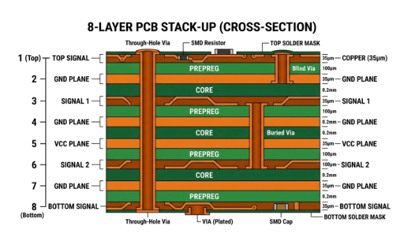
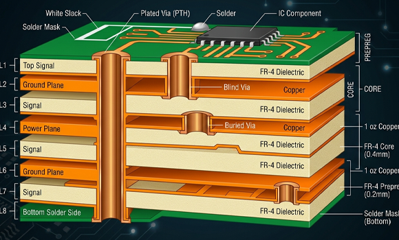

In multilayer PCB design, one of the most overlooked yet critical details is layer orientation. While PCB stack-up defines how layers are arranged, layer orientation ensures that every layer is correctly interpreted during fabrication and assembly.
A simple mistake in orientation—such as a mirrored layer or unclear labeling—can lead to misaligned copper patterns, reversed footprints, and even complete board failure during manufacturing.
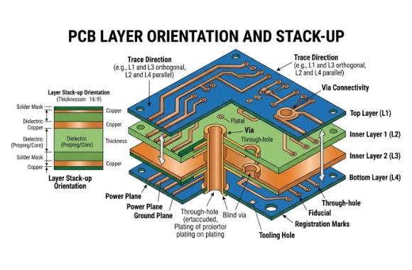
👉 In short, layer orientation is the communication language between PCB designers and manufacturers.
What Is PCB Layer Orientation?
Layer orientation refers to the correct identification and directional definition of each PCB layer within the stack-up, ensuring that top, bottom, and inner layers are properly understood during fabrication.
Although EDA tools define layer order logically, manufacturers rely on physical markers and consistent labeling to confirm orientation during CAM processing.
Without clear orientation reference, even correctly designed Gerber data can be misinterpreted due to mirrored outputs or software export variations.
Why Layer Orientation Matters in PCB Manufacturing
PCB fabrication is not just a digital process—it is a physical stacking and imaging process. Any ambiguity in layer direction introduces risk.
A missing or incorrect orientation reference can result in:
- Mirrored copper layers
- Incorrect stack-up assembly
- Misaligned vias or traces
- Assembly-level failures that cannot be repaired
Because many CAD tools allow mirrored Gerber export, manufacturers cannot rely on file naming alone. Physical or copper-based labeling becomes essential for verification.
👉 This is why layer orientation is treated as a DFM-critical requirement, not just a design preference.
How Layer Orientation Is Defined in PCB Design
In professional PCB design practice, orientation is established through a combination of logical stack definition and physical marking strategy.
The top layer is always treated as the reference view. From this perspective, all top-side markings should appear readable, while bottom-layer markings are intentionally mirrored so that they become readable when the board is physically flipped.
For multilayer boards, each internal layer is also assigned a clear identifier, ensuring correct sequencing during lamination and stack-up verification.
The Role of Physical Layer Labeling
Even though modern file formats such as Gerber X2 or ODB++ can embed layer metadata, physical labeling remains essential in real manufacturing environments.
Engineers typically embed simple identifiers such as “TOP”, “BOT”, or layer numbers directly into the copper or documentation layers. This provides a visual and structural reference point during CAM review and fabrication.
More importantly, copper-based labeling is preferred because it remains visible throughout early fabrication stages, unlike silkscreen or documentation layers that appear later in the process.
Multilayer PCB Considerations
As PCB complexity increases, layer orientation becomes even more critical. In multilayer stack-ups, any inversion of inner layers can result in functional failures that are extremely difficult to detect after lamination.
To avoid this, manufacturers rely on consistent labeling strategies across all layers, often combined with stack-up visualization patterns or edge markers.
This ensures that every layer is assembled in the correct sequence and orientation before pressing and drilling processes begin.
Best Practices for Layer Orientation Control
A robust PCB design workflow treats layer orientation as part of DFM rather than documentation. Professional design teams typically ensure that:
- Top and bottom layers always follow a consistent viewing convention
- Copper-layer labels are added for verification
- Inner layers are clearly numbered in stack-up order
- Gerber export settings are reviewed to prevent accidental mirroring
These practices significantly reduce fabrication ambiguity and eliminate one of the most common causes of engineering holds during CAM review.
Conclusion
PCB layer orientation is not just a labeling convention—it is a critical manufacturing control mechanism.
While modern PCB tools define layer structure digitally, real-world fabrication still depends on clear, physical, and unambiguous orientation references to ensure stack-up accuracy and assembly success.
👉 In advanced PCB manufacturing, correct layer orientation is what separates a clean build from a costly fabrication error.
Ready for Production? Kickstart Your Project Now. info@ysx-tech.com
Unsure About the Design? Consult with Our Lead Engineers Today. contact us
Share on Social:


