




Automated X-Ray Inspection (AXI) in PCB Assembly
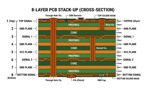
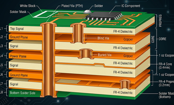
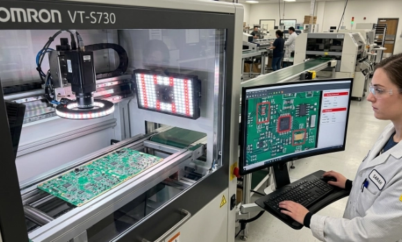

Automated X-Ray Inspection (AXI) is a non-destructive inspection technology used to evaluate hidden solder joints and internal structures of PCB assemblies.
Unlike optical inspection systems, AXI penetrates through materials using X-ray radiation, making it indispensable for modern electronics where components such as BGA, CSP, QFN, and flip-chip packages conceal solder joints beneath the device body.
As PCB designs move toward higher density and smaller pitch, AXI has become a critical quality assurance step in automotive, aerospace, medical, and high-speed computing industries.
Working Principle of AXI
AXI is based on the principle of differential X-ray absorption:
- Dense materials (solder, copper) absorb more radiation → appear darker
- Less dense materials (air voids, resin) absorb less → appear brighter
The system captures these differences to reconstruct internal structures.
Key imaging mechanisms:
- Transmission imaging (2D)
- Oblique angle imaging (2.5D)
- Computed tomography (3D CT reconstruction)
AXI System Architecture
A complete AXI system includes:
- X-ray source tube
- Detector (flat panel / image intensifier)
- Motion control stage
- Image processing software
- AI defect recognition module (advanced systems)
Manufacturing Defects Detected by AXI
AXI is specifically designed to detect hidden structural and solder-related defects, including:
Solder joint defects:
- Voids (gas entrapment inside solder)
- Head-in-pillow (BGA separation defect)
- Cold solder joints
- Insufficient wetting
Structural defects:
- BGA misalignment
- Bridging under components
- Internal layer voids in some stackups
Critical insight:
These defects are not visible under AOI or visual inspection, making AXI essential.
AXI vs AOI (Critical Comparison)
| Feature | AXI | AOI |
|---|---|---|
| Inspection Type | Internal (3D/2D) | Surface |
| Technology | X-ray imaging | Optical imaging |
| Hidden solder joints | Detectable | Not detectable |
| Speed | Slower | Faster |
| Cost | Higher | Lower |
| Application | High reliability PCBA | General SMT inspection |
👉 Industry rule: AOI + AXI = complete inspection coverage
AXI Inspection Methods
1. 2D AXI
- Fast imaging
- Used for production screening
- Limited depth interpretation
2. 2.5D AXI
- Tilted imaging improves defect visibility
- Common in SMT production lines
3. 3D CT AXI
- Full volumetric reconstruction
- Used for failure analysis and aerospace-level validation
AXI Process Flow in Manufacturing
- PCB assembly completed (SMT reflow)
- PCB enters inspection stage
- AXI scanning performed
- Image reconstruction
- Automated defect detection
- Engineer validation
- Quality report generation
Design for Inspection (DFI Considerations)
To ensure AXI effectiveness:
- BGA pad design must allow void visibility
- Avoid overlapping high-density copper shadows
- Ensure consistent solder volume
- Maintain proper component spacing for imaging clarity
IPC and Industry Standards
AXI is aligned with:
- IPC-A-610 (acceptability of electronic assemblies)
- IPC-7095 (BGA assembly guidelines)
- IPC-6012 (PCB performance standard)
For automotive and aerospace:
- ISO 26262 (functional safety)
- AS9100 (aerospace quality system)
Limitations of AXI
Despite its advantages:
- High equipment cost
- Slower than AOI
- Requires skilled interpretation in complex cases
- Shadow overlap in dense assemblies may affect clarity
Ready to implement X-ray inspection in your PCB assembly process?
Choosing the right inspection system is critical to ensuring product quality and yield. YSX provides expert guidance and tailored X-ray inspection solutions—ranging from streamlined 2D systems to advanced 3D CT technology—to meet your specific application needs.
Ready for Production? Kickstart Your Project Now. info@ysx-tech.com
Unsure About the Design? Consult with Our Lead Engineers Today. contact us
Share on Social:


