




PCB Panel Creation Explained: Process, Methods, and Design Best Practices

Introduction
In PCB manufacturing, efficiency is everything.
Producing individual boards one by one is not only inefficient but often impractical for automated assembly.
This is where PCB panel creation (panelization) comes in.
By combining multiple boards into a single panel, manufacturers can significantly improve production efficiency, reduce handling complexity, and optimize overall cost.
👉 In modern electronics manufacturing, panel creation is not optional—it is a standard engineering practice.
What Is PCB Panel Creation?
PCB panel creation is the process of arranging multiple individual circuit boards into a single larger panel for fabrication and assembly.
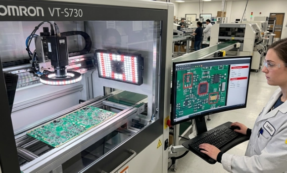
Instead of processing each PCB separately, manufacturers produce them together as an array, allowing the entire panel to move through drilling, etching, SMT placement, and reflow processes as one unit.
After assembly, the boards are separated through a process called depanelization.
👉 In simple terms:
Panel creation turns multiple small boards into one manufacturable unit.
Why PCB Panel Creation Matters
Panelization is not just about grouping boards—it directly impacts manufacturing efficiency and product quality.
By using panels, manufacturers can:
- Improve throughput in automated assembly lines
- Reduce manual handling and positioning errors
- Increase mechanical stability during SMT processes
- Optimize material utilization and reduce waste
More importantly, small or irregularly shaped PCBs cannot be processed efficiently without panelization. Panels provide the structural support required for automated equipment.
👉 Without proper panel design, even a perfect PCB layout may fail in production.
How PCB Panel Creation Works
Panel creation begins after the PCB layout is finalized. Engineers arrange multiple PCB units into an array while considering spacing, breakaway methods, and assembly constraints.
The panel typically includes additional structural elements such as rails, tooling holes, and fiducials to support automated assembly.
Once designed, the entire panel goes through fabrication and assembly as a single unit. Only after all processes are completed are the individual boards separated.
👉 The goal is simple:
maximize efficiency during manufacturing, then separate cleanly at the end.
Common PCB Panelization Methods
V-Scoring (V-Cut)
V-scoring uses a V-shaped groove along straight lines between boards, allowing them to be easily separated after assembly.
It is ideal for rectangular boards and offers high panel density with minimal spacing. However, it is limited to straight-line designs and may introduce mechanical stress during separation.
Tab Routing (Mouse Bites)
Tab routing uses small connecting tabs with perforations to hold boards together during production.
This method supports complex board shapes and irregular outlines, making it more flexible than V-scoring. After assembly, boards are snapped off and edges are cleaned if necessary.
👉 In practice:
- V-score = high efficiency, simple geometry
- Tab routing = flexibility, complex shapes
Key Design Considerations for Panel Creation
Effective panel design requires balancing manufacturability, cost, and mechanical stability.
Engineers must consider factors such as panel strength, spacing between boards, and the placement of sensitive components near edges. Improper panelization can lead to warpage, assembly defects, or damage during depanelization.
Panel size must also match manufacturing equipment constraints, ensuring compatibility with SMT lines and conveyor systems.
👉 A well-designed panel improves yield.
👉 A poor panel design creates hidden production risks.
Engineering Challenges in Panel Design
Panel creation is not just a layout task—it is an engineering optimization problem.
Designers must carefully manage:
- Mechanical stress during depanelization
- Warpage during reflow
- Component clearance near breakaway edges
- Panel rigidity vs. ease of separation
These trade-offs require experience and close coordination between design and manufacturing teams.
Manufacturing Capability Matters
Panelization quality depends heavily on manufacturing capability.
A capable PCB manufacturer can:
- Optimize panel layout for cost and yield
- Select the appropriate depanelization method
- Ensure compatibility with automated assembly
- Reduce material waste and improve efficiency
👉 Panel creation is not just design—it is DFM in action.
Conclusion
PCB panel creation is a fundamental part of modern electronics manufacturing. It transforms individual PCB designs into production-ready arrays that improve efficiency, reduce cost, and enable automated assembly.
From method selection to structural optimization, every detail in panel design impacts final product quality.
Ready for Production? Kickstart Your Project Now. info@ysx-tech.com
Unsure About the Design? Consult with Our Lead Engineers Today. contact us
Share on Social:


