




What Is PCB Layout and Design?
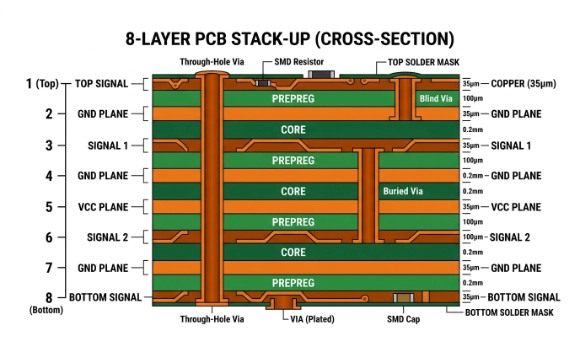
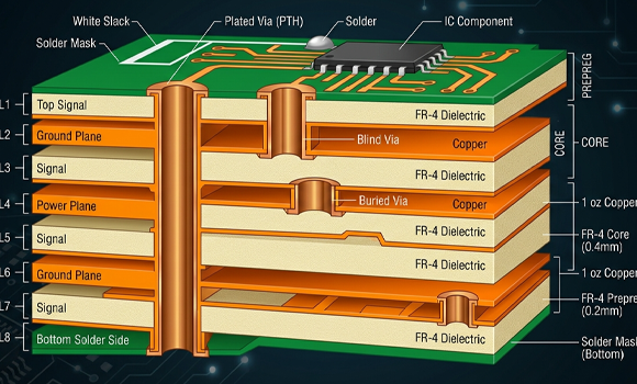

PCB layout and design is the process of converting a schematic into a manufacturable printed circuit board. It determines not only whether the circuit works, but also its performance, reliability, and production efficiency.
In essence:
Design defines functionality, while layout defines performance and manufacturability.
Some popular PCB design software
- Spring Layout
- Protel
- Eagle
- Allego Cadance
- OrCAD
- Proteus
- EasyEDA
- Altium Designer
- DesignSpark
- KiCAD
A vast array of software options exists for PCB design, each with its unique architecture and specialized capabilities. Choosing the right tool is a strategic decision; engineers must evaluate whether a platform aligns with their specific project requirements—such as the complexity of multi-layer vs. single-layer layouts. Beyond technical features, the software’s intuitive usability and its ability to scale with demanding design constraints are critical factors to consider before integration into the workflow.
PCB Layout and Design Process
1. Requirement Definition: The Starting Point of Everything
PCB design does not begin with drawing circuits. It begins with understanding the product itself. Engineers must define what the product needs to achieve, the environment it will operate in, performance expectations such as speed and power consumption, as well as constraints like size and cost.
Although this stage may seem abstract, it actually sets the boundaries for the entire design process. If requirements are not clearly defined, even a well-executed design can lead to costly redesigns later.
2. Schematic Design: From Function to Circuit Logic
Once requirements are defined, the process moves into circuit design. Engineers select core components, build power architectures, and establish complete electrical connections based on functional needs.
At this stage, the focus is not on physical layout but on ensuring correct circuit logic. A well-designed schematic guarantees that all functional blocks operate as intended and form a stable system foundation.
3. PCB Structure Planning: Defining the Physical Framework
After the circuit logic is completed, the next step is to define how the board will physically exist. PCB structure planning translates logical design into physical constraints, including layer stack-up, board dimensions, interface placement, and functional zoning.
In high-speed or high-density designs, this step becomes especially critical. Decisions such as separating analog and digital domains or maintaining continuous power planes are locked in at this stage and directly influence final performance.
4. PCB Layout: The Most Critical Stage for Performance
Layout is one of the most important steps in the entire PCB design process. Engineers determine component placement while considering signal paths, functional grouping, and electromagnetic interference control.
A good layout is not about visual arrangement—it is about performance optimization. The shortest critical paths, minimal interference, and proper thermal distribution all contribute to system stability. In many high-performance designs, the final product quality is largely determined at this stage.
5. PCB Routing: Connecting the Circuit
After layout, the design enters the routing stage. This is where electrical connections between components are physically implemented using copper traces while maintaining signal integrity.
High-speed signals require controlled impedance, power networks must remain stable with low noise, and return paths must be carefully managed. Poor routing can cause instability even if the schematic and layout are correct.
6. DFM Analysis: Making the Design Manufacturable
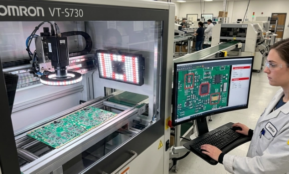
A completed design is not automatically ready for production. Design for Manufacturability (DFM) ensures that the PCB can be reliably manufactured at scale.
This includes verifying whether trace widths are within manufacturing limits, spacing is sufficient, pad designs are compatible with assembly processes, and component footprints match real-world requirements. The goal is simple: prevent production issues before they happen.
7. DFT Design: Ensuring the Product Can Be Tested
Before moving into production, testability must also be considered. Design for Testability (DFT) introduces test points and debugging interfaces that allow functional and automated testing during manufacturing.
Without proper DFT planning, production testing becomes time-consuming and costly, especially in mass production environments.
8. Manufacturing Data Output: Preparing for Production
Once the design is finalized, manufacturing files are generated. These include Gerber files, drill data, BOM (Bill of Materials), and pick-and-place files.
These documents serve as the only communication bridge between design and manufacturing. Any error in this stage can lead to production failure, making verification extremely important.
9. Prototype Validation: The Final Step Before Mass Production
Even a well-designed PCB must be validated through physical prototypes. Engineers perform electrical testing, signal integrity checks, and thermal analysis to ensure real-world performance matches expectations.
Many hidden issues, such as subtle interference or localized heating, only become visible during this stage. Therefore, prototype validation is a critical feedback loop before scaling to mass production.
Why PCB Layout and Design Matter
Not just about function—about success.
A well-executed PCB design can:
Poor design may lead to:
What We Can Do for Your PCB Design Project
From concept to production, we optimize every detail.
- DFM Optimization
Identify and eliminate manufacturability risks early in the design stage - Component Placement & Footprint Optimization
Improve assembly efficiency and reduce defects - High-Speed & High-Density Design Support
Support multi-layer, HDI, and complex PCB structures - Signal & Power Integrity Optimization
Reduce noise, crosstalk, and voltage instability - Thermal & Structural Design Optimization
Prevent overheating and ensure long-term reliability
👉 Our goal:
Not just a working design, but a stable, manufacturable, and scalable solution
Design for Manufacturing Capability
We design with production in mind.
- Standardized design rules for automated assembly
- Full compatibility with SMT and THT processes
- Test point planning for efficient inspection
- Optimized pad and spacing for higher yield
👉 Result:
Higher yield, fewer defects, and consistent production quality
Conclusion
PCB layout and design are not just engineering steps—they are the foundation of a successful product.
Ready for Production? Kickstart Your Project Now. info@ysx-tech.com
Unsure About the Design? Consult with Our Lead Engineers Today. contact us
Share on Social:


