




Blind Vias and Buried Vias: Definition, Differences, and Applications in PCB Design
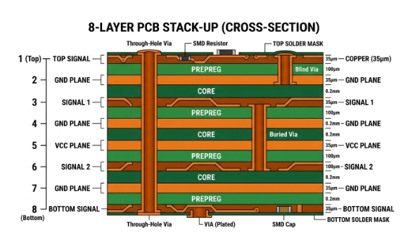
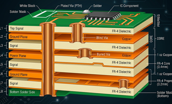

What Are Blind Vias and Buried Vias?
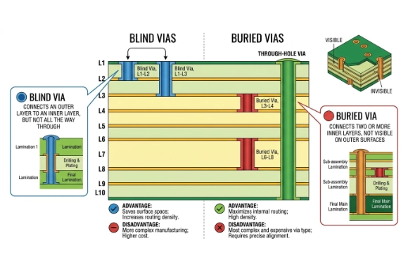
Blind vias and buried vias are advanced types of plated vias used in multilayer printed circuit boards (PCBs) to connect different layers without passing through the entire board.
They are essential in modern electronics where high-density interconnect (HDI) and compact layouts are required.
- Blind vias connect the outer layer to one or more inner layers
- Buried vias connect only internal layers and are not visible externally
What Is a Blind Via?
A blind via is a partial-depth hole that starts from the surface of the PCB and extends to one or more inner layers, but does not go through the entire board.
Key Features:
- Visible from one side (top or bottom)
- Connects outer layers to inner layers
- Commonly used in HDI PCB designs
Advantages:
- Saves surface space for components
- Enables higher routing density
- Reduces signal path length
Limitations:
- Requires precise depth control during drilling
- Limited quantity depending on board thickness
- Higher cost than standard through vias
What Is a Buried Via?
A buried via is a via that connects only inner layers of a PCB and is completely enclosed within the board structure, making it invisible from the outside.
Key Features:
- Not visible externally
- Connects internal layers only
- Used in multilayer PCB stackups
Advantages:
- Maximizes routing space on outer layers
- Improves signal integrity by shortening trace paths
- Reduces noise and crosstalk
Limitations:
- More complex manufacturing process
- Requires layer-by-layer fabrication before lamination
- Higher production cost
Blind Via vs Buried Via: Key Differences
| Feature | Blind Via | Buried Via |
| Visibility | Visible from one side | Completely hidden |
| Connection | Outer layer ↔ inner layers | Inner layers only |
| Manufacturing stage | After stack-up drilling | Before lamination |
| Cost | Medium | Higher |
| Application | Surface routing, HDI | Internal routing optimization |
The main difference lies in which layers are connected and whether the via is visible externally.
Why Use Blind and Buried Vias?
These advanced vias are widely used to solve modern PCB design challenges:
1. Increase PCB Density
They allow more routing channels without increasing board size or layer count.
2. Save Space
By limiting via depth, more surface area is available for components and signal routing.
3. Improve Signal Integrity
Shorter signal paths reduce interference, noise, and crosstalk.
4. Enhance Thermal Management
Vias help transfer heat between layers, improving overall thermal performance.
Manufacturing Process Overview
The fabrication of blind and buried vias involves more complex steps than standard vias:
Blind Vias:
- Drill from outer layer to target inner layer
- Plate with copper (electroplating)
- Ensure accurate depth control
Buried Vias:
- Drill between inner layers before lamination
- Plate the via walls
- Laminate layers together into a full PCB stack
Buried vias must be formed before the board is fully assembled, making them more complex and costly.
Applications of Blind and Buried Vias
These vias are widely used in high-performance electronics:
- HDI PCBs
- Smartphones and tablets
- Networking and communication equipment
- Automotive electronics
- High-speed computing systems
They are especially critical in designs where space is limited and signal performance is critical.
Design Considerations
When designing blind and buried vias, engineers should consider:
- Aspect ratio (depth vs diameter)
- Layer stack-up structure
- Manufacturing capabilities of PCB suppliers
- Cost vs performance trade-offs
Proper planning is essential to avoid fabrication issues and ensure reliability.
Conclusion
Blind vias and buried vias are key technologies in modern PCB design, enabling compact layouts, improved signal integrity, and higher circuit density.
While they increase manufacturing complexity and cost, their benefits make them indispensable in advanced electronics, particularly in HDI and multilayer PCB applications.
Ready for Production? Kickstart Your Project Now. info@ysx-tech.com
Unsure About the Design? Consult with Our Lead Engineers Today. contact us
Share on Social:


