




PCB Side Plating: Definition, Process, Benefits, and Design Guidelines

What Is PCB Side Plating?
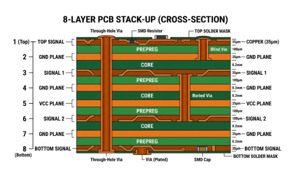
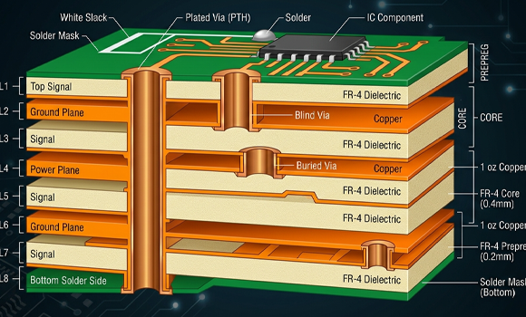
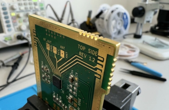
PCB side plating, also known as edge plating, border plating, or castellation, refers to the process of applying a continuous metal (typically copper) layer along the edges of a printed circuit board (PCB).
This plating connects the top and bottom copper layers and extends along one or more board edges, forming a conductive path around the PCB perimeter.
Side plating can be applied to:
- Entire board edges
- Partial outlines
- Internal cutouts or slots
Why Use Side Plating in PCB Design?
Side plating is widely used in advanced PCB designs where electrical performance and mechanical reliability are critical.
Key Benefits:
1. Enhanced Electrical Connectivity
- Creates continuous conductive paths along the board edge
- Enables edge-based electrical connections
- Improves current-carrying capability
2. Improved EMC & EMI Shielding
- Acts like a partial Faraday cage around the PCB
- Reduces electromagnetic interference (EMI)
- Improves electromagnetic compatibility (EMC)
3. Better Signal Integrity
- Reduces signal loss and interference
- Ideal for high-frequency and RF applications
4. Enhanced Thermal Performance
- Edge copper acts as an additional heat dissipation path
- Helps manage temperature in high-power designs
5. Increased Mechanical Strength
- Reinforces PCB edges against stress and vibration
- Improves durability in harsh environments
Common Applications of Side Plating
Side plating is commonly used in:
- RF and high-frequency circuits
- Wi-Fi and Bluetooth modules
- Industrial and automotive electronics
- Board-to-board connections
- PCBs inserted into metal enclosures
It is especially valuable in compact devices where space, shielding, and reliability are critical.
PCB Side Plating Manufacturing Process
The fabrication of side plating requires precise control and additional processing steps:
- Edge routing / milling
- PCB outline is machined before plating
- Surface preparation
- Cleaning and roughening for adhesion
- Electroless copper deposition
- Thin conductive layer applied
- Electroplating
- Builds up copper thickness on edges
- Surface finishing
- ENIG, ENEPIG, or HASL for protection and solderability
PCB Side Plating Design Guidelines
To ensure manufacturability and performance:
- Define metalized areas using overlapping copper in CAD
- Maintain minimum copper overlap (~0.3–0.5 mm)
- Keep ≥0.8 mm clearance on non-connected layers
- Avoid placing internal copper too close to edges
- Clearly specify side plating requirements in fabrication files
Proper design coordination with the PCB manufacturer is essential.
Side Plating vs Castellated Holes
Although related, they serve different purposes:
- Side plating: continuous copper along edges
- Castellated holes: half-holes used for module-to-board soldering
Both can be combined in advanced PCB designs for improved connectivity.
Limitations of Side Plating
Despite its advantages, side plating has some constraints:
- Higher manufacturing complexity and cost
- Requires precise edge preparation
- Not compatible with some panelization methods (e.g., V-cut)
- Requires strict design rules to avoid defects
Conclusion
PCB side plating is an advanced fabrication technique that enhances electrical connectivity, EMI shielding, thermal performance, and mechanical strength.
While it increases manufacturing complexity, it is essential for high-performance applications such as RF modules, HDI designs, and industrial electronics.
For designs requiring edge connections or improved EMC performance, side plating is a highly effective solution.
Ready for Production? Kickstart Your Project Now. info@ysx-tech.com
Unsure About the Design? Consult with Our Lead Engineers Today. contact us


