




PCB Layer Stackup
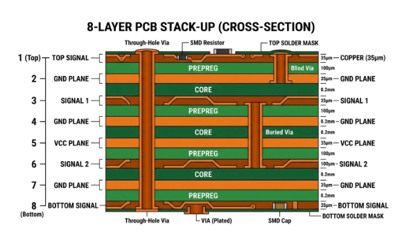
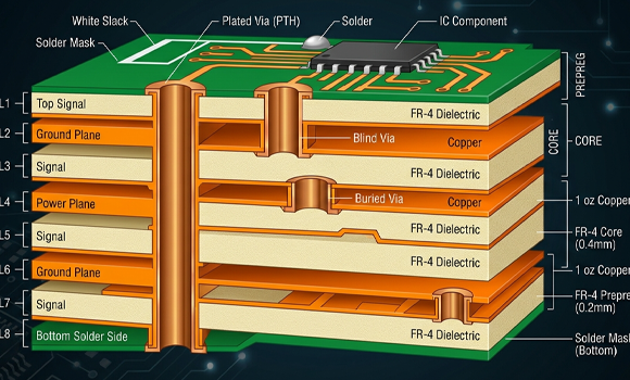

What Is PCB Stackup?
PCB stackup refers to the arrangement of copper layers and insulating materials in a multilayer PCB.
PCB Stack-up Design: The Foundation of High-Performance Electronics
In modern electronics, PCB stack-up design is far more than just layering copper and substrate; it is a critical engineering process that determines Electromagnetic Compatibility (EMC), Signal Integrity (SI), and Power Integrity (PI).
I. The Critical Importance of Stack-up Design
1. Electromagnetic Compatibility (EMC)
A proper stack-up is the key to minimizing differential and common-mode radiation. By reducing the distance between signal traces and their reference planes, you ensure compliance with EMC standards, allowing your device to operate without interfering with—or being affected by—neighboring electronics.
2. Signal Integrity (SI)
A well-structured stack-up ensures constant controlled impedance for signal traces, which drastically reduces reflections and crosstalk. In high-speed digital and RF circuits, even minor signal degradation can lead to data errors or hardware failure.
Expert Insight: In high-density, high-frequency designs, using multiple ground planes (GND) is highly recommended—even if there is only one "type" of ground. This helps minimize loop inductance and provides a stable reference for multiple routing layers.
3. Power Integrity (PI)
By strategically placing power and ground planes close together, a stack-up can reduce plane impedance and voltage fluctuations (ripple). This is essential for complex circuits requiring stable power across multiple voltage domains.
4. Thermal Management
In high-power applications, copper layers act as heat sinks. An optimized stack-up maximizes thermal dissipation efficiency, preventing localized hotspots that can degrade component lifespan or cause catastrophic failure.
II. PCB Classification: Single vs. Multilayer
- Single & Double-Sided PCBs: Suitable for simple, low-frequency applications. While cost-effective, they offer limited EMI protection and routing flexibility.
- Multilayer PCBs: The gold standard for complex, high-speed tasks. By interleaving signal, ground, and power layers, they achieve compact footprints, superior EMI resistance, and diverse routing options. For frequencies above 10 MHz, multilayer boards are mandatory to keep radiation levels within safe limits.
III. Common Stack-up Configurations
1. 4-Layer Stack-up
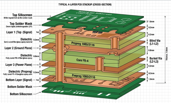
Standard Config: Signal 1 / GND / Power / Signal 2
- Advantage: Tight coupling between signal lines and reference planes reduces loop radiation by approximately 10dB. It also lowers plane impedance, reducing common-mode emissions.
- Enhanced EMI Config:
Signal/Power / GND / GND / Signal/Power- Power is routed as traces on the signal layers. The dual-ground planes provide superior shielding but offer less isolation between different signal levels.
| Parameter | Specification |
| Board Thickness | 1.6 mm |
| Outer/Inner Copper | 1 oz / 0.5 oz (or 1 oz) |
| HDI Technology | None (Standard) |
2. 6-Layer Stack-up
An ideal balance between cost and performance for mid-range precision electronics.
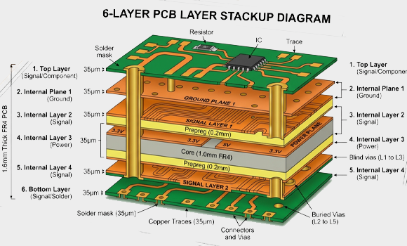
Typical Layout: S1 / GND / S2 / S3 / Power / S4
- Value: Effectively separates signal layers to minimize interference. The ground planes serve as low-noise return paths and provide excellent Electrostatic Discharge (ESD) protection.
3. 8-Layer Stack-up
Used when maximum signal shielding and performance are required for high-speed communication.
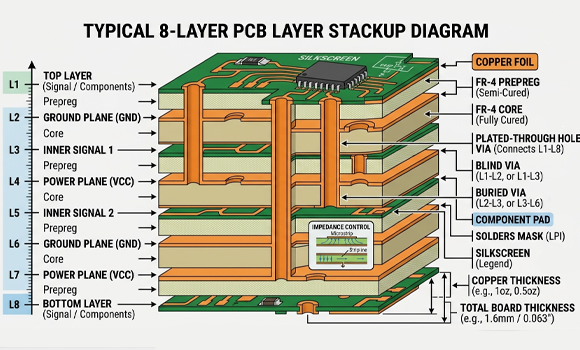
High-Performance Layout: LS Signal / Power / GND / HS Signal / HS Signal / GND / Power / LS Signal
- Technical Edge: This topology provides excellent EMI performance, low ground impedance, and highly effective shielding for differential pairs.
4. 10-Layer Stack-up
Designed for the most demanding applications, such as core switches and high-end computing.
Typical Layout: GND / S(H) / S(V) / GND / S(H) / S(V) / Power / S(H) / S(V) / GND
- Key Benefit: Superior isolation for designs requiring six routing layers. It utilizes Orthogonal Routing (alternating Horizontal and Vertical traces on adjacent layers) to eliminate crosstalk.
YSX Manufacturing Services at a Glance
1. Advanced PCB Fabrication Capabilities
From standard boards to high-complexity designs, YSX delivers precision-engineered PCBs tailored to your specifications.
- Versatile Layers: Support for 1–32 layers.
- Specialized Types: Expertise in Rigid, Flex, Rigid-Flex, HDI, and Metal-Core (MCPCB).
- Precision Engineering: Controlled impedance, blind/buried vias, via-in-pad, and back-drilling technology.
- Premium Finishes: Multiple surface treatments including OSP, ENIG, HASL, Immersion Silver, and Gold.
- Rigorous Standards: IPC Class 2/3 compliance with ISO, IATF 16949, UL, RoHS, and REACH certifications.
2. Rapid PCB Prototyping
Accelerate your R&D cycle with our agile prototyping service. We bridge the gap between initial concept and pilot production with:
- Fast-Turn Delivery: Swift turnaround for single boards to small batches.
- Seamless Quoting: Instant online pricing and professional stack-up guidance.
- Design Validation: Helping you iterate faster with production-grade prototypes.
3. Professional PCB Assembly (PCBA)
YSX offers high-reliability assembly services, managing the complexity of modern electronics.
- Flexible Models: Full Turnkey, Consigned, or Mixed-material assembly.
- Advanced SMT: Capability for 01005 passives, ultra-fine-pitch BGAs, and THT (Through-hole) mounting.
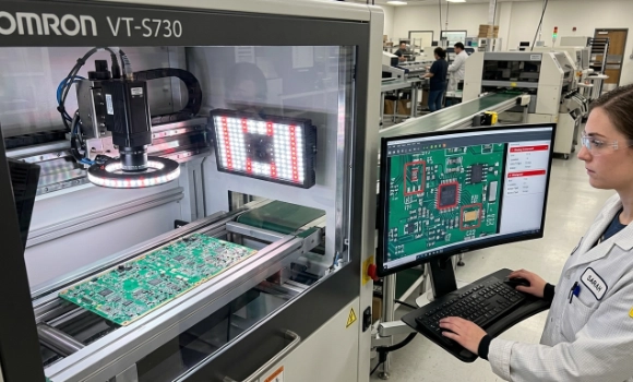
- Total Quality Control: Integrated X-ray (for BGA), AOI inspection, and comprehensive functional testing.
- Rapid Fulfillment: Optimized workflows ensuring industry-leading lead times.
4. Strategic BOM & Sourcing Services
Optimize your supply chain with our intelligent component management.
- Smart Sourcing: Global procurement with a focus on cost-effectiveness and lead-time optimization.
- Lifecycle Management: Proactive checks for EOL (End of Life) and NRND (Not Recommended for New Design) components.
- Risk Mitigation: Expert identification of high-quality, drop-in substitutes to prevent production delays.
5. Complimentary DFM Excellence
We don't just build; we optimize. YSX provides a Free DFM (Design for Manufacturability) Check for every project.
- Engineer-Led Review: A combination of automated tools and veteran engineer scrutiny.
- Comprehensive Audit: Validation of stack-up, impedance, clearances, drill registration, and solderability.
- Actionable Feedback: Receive clear, technical reports to fix potential issues before fabrication starts, ensuring a "First Time Right" manufacturing experience.
Ready for Production? Kickstart Your Project Now. info@ysx-tech.com
Unsure About the Design? Consult with Our Lead Engineers Today. contact us


