




What is HDI PCB
HDI PCBs are engineered for miniaturization, utilizing advanced interconnect technologies to maximize circuit density within extremely limited spaces. By incorporating microvias, blind and buried vias, and fine-line routing, HDI boards significantly increase wiring density compared to traditional PCBs, ultimately enabling the development of smaller, more powerful electronic devices.
High-Density Interconnect (HDI) PCBs are typically defined by a line width/spacing (L/S) of ≤ 0.10mm and microvia diameters of ≤ 0.15mm. This technology achieves interlayer connectivity through the sequential stacking of conductive and insulating layers, interconnected by precision microvias (including blind and buried vias). Consequently, the HDI manufacturing process is widely recognized in the industry as Build-Up Process (BUP) or Build-Up Multilayer (BUM) technology.
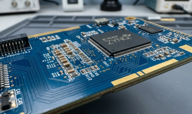
Our HDI PCB Capabilities
YSX supports advanced HDI PCB fabrication for high-density and high-performance designs.
| Capability Category | YSX Capability |
| HDI Types | HDI I, II, III, Any-layer HDI |
| Stack-ups | 1+n+1, 2+n+2, 3+n+3 |
| Layer Count | Up to 32 layers |
| Microvia Size | 0.075 – 0.15 mm |
| Min Trace / Space | 2/2 – 3/3 mil |
| Via Types | Microvias, blind, buried, via-in-pad |
| Materials | High-TG, high-speed, high-frequency |
| Surface Finish | ENIG, Immersion Gold, OSP |
| Advanced Processes | Filled vias, stacked vias, HDI lamination |
| Production | Prototype to mass production |
Typical reference:
- Prototype lead time: 8–14 days
- Cost increases with layer count and stack-up complexity
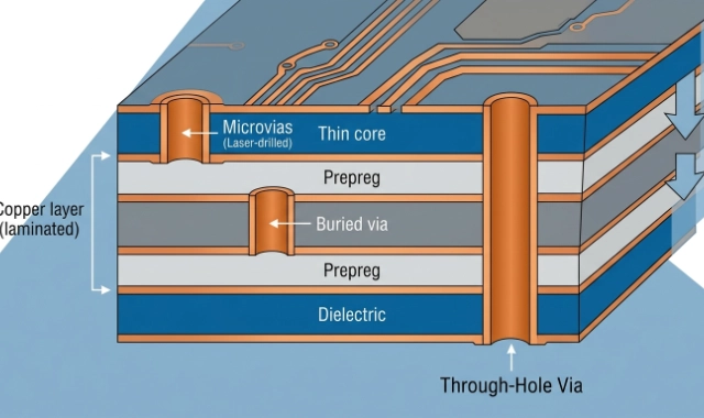
HDI PCB Stack-up Structures
Different stack-up configurations determine HDI complexity, performance, and cost.:
- 1+n+1 (HDI I) → Basic HDI structure
- 2+n+2 (HDI II) → Higher density and complexity
- 3+n+3 (HDI III) → Advanced high-density design
These structures are built using sequential lamination processes, increasing design flexibility but also manufacturing complexity.
Key Features of HDI PCB
HDI technology combines multiple advanced fabrication techniques to achieve miniaturization and performance.
- Microvias (≤0.15mm) → Enable high-density routing
- Blind & Buried Vias → Optimize layer interconnection
- Fine Trace & Spacing → Typically ≤4mil
- Sequential Lamination → Multi-step precision manufacturing
- Via-in-Pad Technology → Support BGA and fine-pitch components
HDI PCB Types & Classes
HDI PCBs are classified based on structure complexity and lamination cycles.
| Type / Class | Description |
| HDI Type I | Microvias + through holes |
| HDI Type II | Includes buried vias |
| HDI Type III | Complex stacked microvias |
| HDI Class I–III | Defined by lamination cycles |
HDI PCB vs Standard PCB
HDI PCBs provide higher density and performance compared to traditional PCBs.
| Feature | Standard PCB | HDI PCB |
| Via Type | Through-hole | Microvia + blind/buried |
| Density | Low | Very high |
| Size | Larger | Compact |
| Performance | Standard | High-speed capable |
| Cost | Lower | Higher |
| Application | General electronics | High-end devices |
What YSX Can Do for HDI PCB Project
Frequently Asked Questions
Looking For a Reliable HDI PCB Manufacturer?
Contact YSX today to receive a quick quote and expert engineering support, and unlock high-quality PCB manufacturing services.