





What Is DFA in Design for Manufacturing and Assembly?
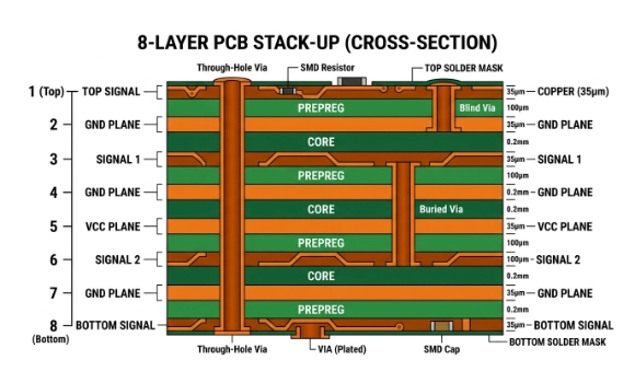
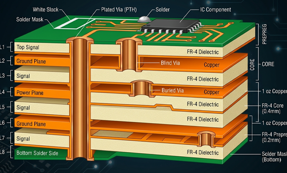

In modern electronics manufacturing, having a functional design is no longer enough. A PCB that works in theory may still fail during production due to assembly challenges, increased costs, or low yield.
To address this, engineers rely on structured methodologies such as DFM (Design for Manufacturing) and DFA (Design for Assembly)—two critical pillars under the broader concept of DFMA (Design for Manufacturing and Assembly).
Among them, DFA focuses specifically on optimizing how easily a product can be assembled, ensuring efficiency, consistency, and cost control.
What Is DFA (Design for Assembly)?
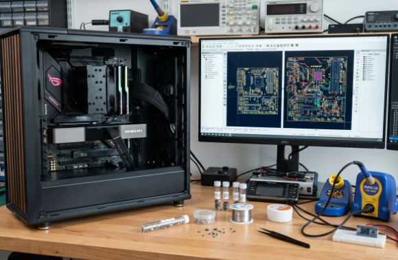
Design for Assembly (DFA) is the process of designing a product in a way that simplifies and optimizes the assembly process. It focuses on reducing complexity, minimizing assembly time, and lowering labor costs from the early design stage.
In PCB manufacturing, DFA ensures that components can be:
- Easily placed
- Correctly oriented
- Reliably soldered
- Efficiently inspected
In simple terms:
👉 DFA makes sure your design is easy to build, not just possible to build.
DFA vs DFM: What’s the Difference?
Although DFA and DFM are closely related, they focus on different stages of production.
| Aspect | DFM (Design for Manufacturing) | DFA (Design for Assembly) |
| Focus | Fabrication of PCB | Assembly of components |
| Goal | Reduce manufacturing complexity | Simplify assembly process |
| Key Concern | Materials, stack-up, tolerances | Placement, orientation, soldering |
| Outcome | High fabrication yield | Faster, error-free assembly |
A PCB design that passes DFM checks may still fail during assembly if DFA is ignored.
Why Is DFA Important in PCB Assembly?
Assembly is often one of the most time-consuming and costly stages in PCB production. Poor design decisions can lead to:
- Increased assembly time
- Higher defect rates
- Rework and delays
- Higher production costs
DFA helps eliminate these issues by optimizing the design early. It can:
- Reduce assembly steps
- Improve automation compatibility
- Increase production yield
- Shorten time-to-market
Key Principles of DFA in PCB Design
1. Reduce Component Count
Fewer components mean:
- Fewer placement operations
- Lower failure probability
- Faster assembly
2. Standardize Components
Using standard packages and footprints helps:
- Improve sourcing flexibility
- Simplify assembly processes
- Reduce errors
3. Optimize Component Placement
Proper placement is critical for automated assembly:
- Maintain consistent orientation
- Ensure adequate spacing
- Group functional components together
This improves pick-and-place efficiency and reduces placement errors.
4. Ensure Clear Polarity and Marking
Incorrect polarity is a common cause of assembly defects.
DFA requires:
- Clear silkscreen markings
- Visible pin-1 indicators
- Consistent orientation
5. Design for Automated Assembly
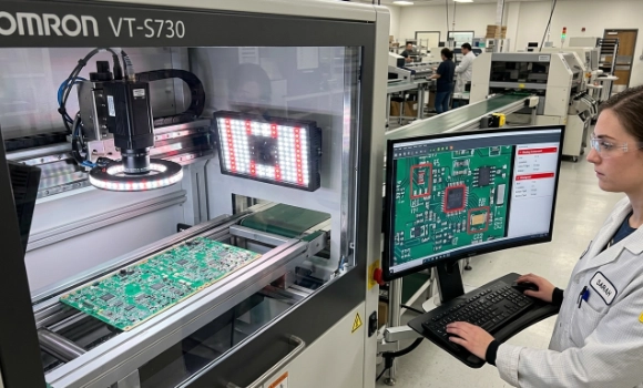
Modern PCB assembly relies heavily on SMT machines. DFA must consider:
- Nozzle clearance
- Component height differences
- Avoiding shadowing effects
6. Provide Proper Fiducials and Alignment Features
Fiducial marks help machines align accurately during assembly, improving placement precision and yield.
Common DFA Issues in PCB Design
Ignoring DFA can result in several real-world problems:
- Component misalignment
- Tombstoning (uneven soldering)
- Solder bridges
- Difficult inspection (hidden joints)
- Increased manual rework
These issues often appear during mass production—not during prototyping.
DFA in the PCB Assembly Workflow
DFA is not a single step—it is integrated throughout the design and production process:
- Design Stage
Engineers optimize layout for assembly - Pre-production Review
Manufacturers verify BOM, footprints, and placement data - Assembly Preparation
Process parameters and tooling are validated - Mass Production
DFA ensures stable, repeatable assembly performance
Best Practices for Applying DFA
To achieve efficient PCB Assembly, consider the following:
- Validate footprints with datasheets
- Maintain consistent component orientation
- Ensure adequate spacing for machines
- Optimize solder paste design
- Include test points for inspection
- Collaborate with manufacturers early
Conclusion
Design for Assembly (DFA) is a critical discipline that ensures your PCB design can be assembled efficiently, reliably, and cost-effectively.
While DFM ensures that a PCB can be manufactured, DFA ensures that it can be assembled smoothly on real production lines. Together, they form the foundation of successful electronics manufacturing.
Ready for Production? Kickstart Your Project Now. info@ysx-tech.com
Unsure About the Design? Consult with Our Lead Engineers Today. contact us
Share on Social:


