




PCB Assembly Guide: Everything You Need to Know About PCBA
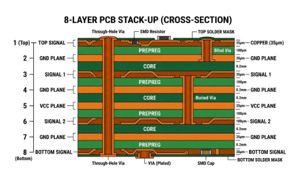
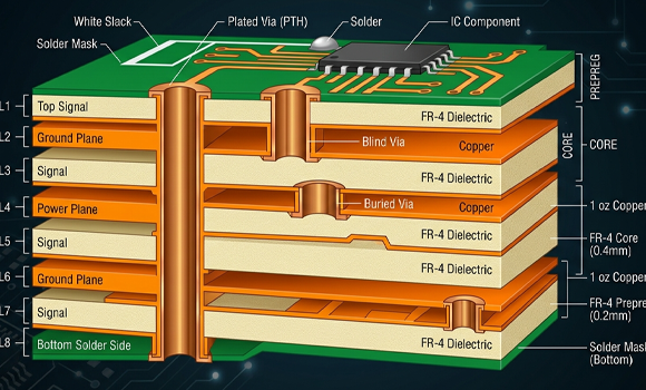

PCB assembly (PCBA) is the process of transforming a bare printed circuit board into a fully functional electronic system. Whether you're developing consumer electronics, industrial equipment, or IoT devices, understanding PCB assembly is essential for ensuring product performance, reliability, and manufacturability.
This guide provides a complete overview of PCB assembly, including its processes, technologies, required files, and key considerations.
Key Files Required for PCB Assembly
Before starting PCB assembly, manufacturers require several essential files:
1. Gerber Files
Gerber files define the physical layout of the PCB, including copper layers, solder mask, silkscreen, and board outline.
2. Bill of Materials (BOM)
The BOM lists all components required for assembly, including part numbers, quantities, and specifications.
3. Pick and Place File
This file provides the exact coordinates and orientation of each component for automated assembly machines.
Types of PCB Assembly Technologies
1. Surface Mount Technology (SMT)
SMT is the most commonly used PCB assembly method in modern electronics.
Features:
- Components mounted directly on PCB surface
- High-speed automated placement
- Suitable for high-density designs
2. Through-Hole Technology (THT)
THT involves inserting component leads into drilled holes and soldering them.
Features:
- Strong mechanical connections
- Better for high-stress or high-power applications
3. Mixed Assembly
Most real-world products use a combination of SMT and THT to balance performance and reliability.
PCB Assembly Process Step-by-Step
A typical PCB assembly workflow includes the following stages:
1. Solder Paste Printing
A stencil is used to apply solder paste onto PCB pads accurately.
2. Component Placement
Automated pick-and-place machines position components based on design data.
3. Reflow Soldering
The board is heated in a controlled temperature profile to melt solder and form connections.
4. Through-Hole Insertion & Wave Soldering
THT components are inserted and soldered using wave soldering.
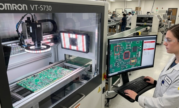
5. Inspection and Quality Control
Common inspection methods include:
- AOI (Automated Optical Inspection)
- X-ray inspection (for BGA, hidden joints)
- Manual inspection
6. Functional Testing
The assembled PCB is tested to ensure it performs as intended in real-world conditions.
Common PCB Assembly Defects
Even with advanced processes, defects can occur:
- Solder bridging (short circuits)
- Cold solder joints
- Component misalignment
- Tombstoning (component lifting)
- Open circuits
Understanding these issues helps improve yield and reduce rework.
Key Factors Affecting PCBA Quality
1. Design for Manufacturing (DFM)
Poor PCB design can lead to assembly failures. DFM ensures:
- Proper pad spacing
- Adequate solder mask
- Manufacturable layouts
2. Component Availability
Supply chain issues can delay production or force substitutions.
3. Process Control
Critical parameters include:
- Reflow temperature profile
- Placement accuracy
- Solder paste quality
4. Testing Strategy
A strong testing plan reduces field failures and improves reliability.
Applications of PCB Assembly
PCB assembly is widely used in:
- Consumer electronics
- Automotive systems
- Medical devices
- Industrial automation
- Telecommunications and IoT
Tips for Choosing a PCB Assembly Manufacturer
When selecting a PCBA partner, consider:
- Manufacturing capability (SMT lines, automation level)
- Quality certifications (ISO, IPC standards)
- Turnaround time (prototype vs mass production)
- Component sourcing capability
- Engineering support (DFM, DFT)
Conclusion
PCB assembly is a critical stage in electronics manufacturing that directly impacts product quality and performance. By understanding the assembly process, technologies, and key considerations, engineers and businesses can significantly improve product reliability and reduce production risks.
Share on Social:


