




What is High-Frequency PCB
A PCB designed for RF and microwave signals where signal loss and dielectric stability are critical.
High-frequency PCBs operate typically above 1GHz and are widely used in RF and microwave applications. These boards require specialized materials with low dielectric constant (Dk) and low loss factor (Df) to ensure signal integrity and minimize transmission loss.
Key Electrical Requirements
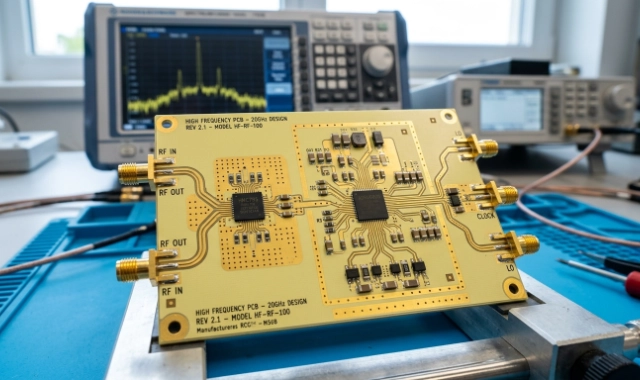
Material and electrical properties directly determine signal quality at high frequencies.
- Low Dielectric Constant (Dk) → Faster signal transmission
- Low Dissipation Factor (Df) → Reduced signal loss
- Stable Thermal Performance → Prevent signal drift
- Low Water Absorption → Maintain performance in humid environments
Our High-Frequency PCB Capabilities
YSX supports advanced RF PCB manufacturing with specialized materials and precision processes.
| Capability Category | YSX Capability |
| Layer Count | 1–20 layers |
| Materials | Rogers, PTFE, Taconic, Ceramic |
| Frequency Range | Up to 100 GHz |
| Dk / Df Control | Low-loss material support |
| Impedance Control | ±5% tolerance |
| Min Trace / Space | 2/2 – 3/3 mil |
| Surface Finish | ENIG, Immersion Silver |
| Via Types | Blind, buried, microvias |
| Special Processes | Backdrilling, via filling |
| Thermal Management | Metal base / hybrid stack-up |
High-Frequency PCB Materials
Material selection is the most critical factor in RF PCB performance.
🔹 Rogers (PTFE-based)
- Ultra-low loss
- Stable dielectric constant
- Ideal for RF & microwave
🔹 PTFE (Teflon)
- Best electrical performance
- Suitable for >10GHz applications
- Higher cost
🔹 Ceramic Substrates
- Excellent thermal conductivity
- High reliability
🔹 High-Speed FR4 (Enhanced)
- Cost-effective alternative
- Suitable for mid-frequency range
Challenges in High-Frequency PCB Design
High-frequency PCB design requires precise control over materials, layout, and manufacturing.
| Challenge | YSX Solution |
|---|---|
| Signal Loss | Low-Df materials + smooth copper |
| Impedance Mismatch | Precise impedance control |
| EMI Interference | Optimized layout & shielding |
| Thermal Instability | Advanced materials & stack-up |
| Manufacturing Difficulty | Experienced engineering support |
High-Frequency PCB Routing Principles
In high-frequency environments, PCB traces, vias, and corners act as distributed circuits with specific impedance, capacitance, and inductance. Even minor routing errors can lead to signal degradation, electromagnetic interference (EMI), or system failure. To ensure Signal Integrity (SI), we adhere to the following eight core routing principles:
When to Choose High-Frequency PCB
High-frequency PCBs are essential for RF and microwave applications.
Choose high-frequency PCB when your project involves:
- RF or microwave signals
- Frequencies above 1 GHz
- Wireless communication systems
- Low signal loss requirements
Why Choose us
Frequently Asked Questions
Looking For a Reliable High-Frequency PCB Manufacturer?
Contact YSX today to receive a quick quote and expert engineering support, and unlock high-quality PCB manufacturing services.