




What is a High-Speed PCB?
High-speed PCBs are engineered to preserve signal integrity in high-frequency and high-data-rate environments.
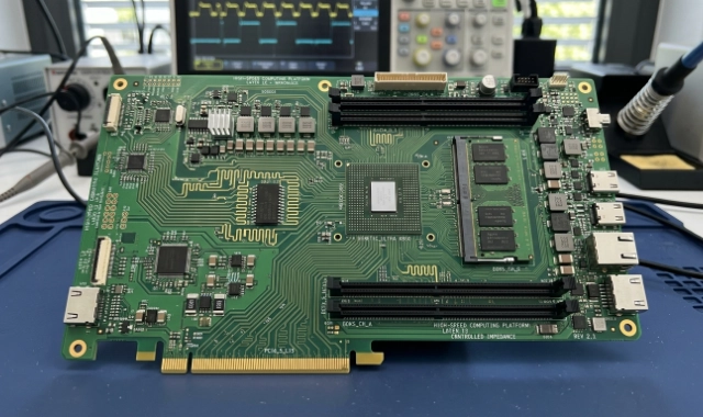
High-speed PCBs are designed to handle fast digital and RF signals while minimizing signal loss, electromagnetic interference (EMI), and distortion. These designs must consider transmission line effects, impedance control, and material properties.
Typical high-speed conditions include:
- Digital signals above 50–100 MHz
- Rise/fall time below 1 ns
- RF signals above 300 MHz
Why High-Speed PCB Design
- 🔹 Signal Integrity (SI)
- Minimize signal reflection and distortion
- Maintain clean waveform transmission
- 🔹 Power Integrity (PI)
- Stable power distribution
- Reduced noise and voltage fluctuation
- 🔹 EMI Control
- Reduce electromagnetic interference
- Improve system reliability
- 🔹 High Data Rate Support
- Support interfaces like PCIe, DDR, HDMI, USB
Key Technologies for High-Speed PCB
Advanced fabrication technologies are essential to ensure signal integrity in high-speed designs.
- Impedance Control → Accurate trace tuning & verification
- Backdrilling → Reduce signal reflection from vias
- Low-Loss Materials → Minimize signal attenuation
- Smooth Copper Foil → Reduce skin effect loss
- Via Filling & Optimization → Improve high-frequency performance
These techniques help maintain signal quality in multi-gigabit systems
General-Purpose High-Speed Interface
Modern electronic systems rely on high-speed interfaces for data transmission.
| Interface | Speed | Application |
|---|---|---|
| USB 3.2 | Up to 10 Gbps | Storage, docking |
| USB4 / Thunderbolt | Up to 40 Gbps | High-speed connectivity |
| HDMI 2.1 | Up to 48 Gbps | 4K/8K video |
| PCIe 4.0 / 5.0 | Up to 32 Gbps/lane | GPUs, SSDs |
| DDR5 | ~50 GB/s | Memory systems |
| Ethernet (10G/100G) | Up to 100 Gbps | Data centers |
Our High-Speed PCB Capabilities
YSX provides advanced manufacturing capabilities tailored for high-speed signal performance.
| Capability Category | YSX Capability |
| Layer Count | Up to 32 layers |
| Stack-up | Custom multilayer stack-ups |
| Materials | Low-Dk / Low-Df laminates (Rogers, Isola, etc.) |
| Signal Speed Support | Up to 56 Gbps |
| Impedance Control | Single-ended & differential |
| Min Trace / Space | 2/2 – 3/3 mil |
| Surface Finish | ENIG, Immersion Silver, OSP |
| Via Technology | Blind, buried, microvias |
| Advanced Processes | Backdrilling, filled vias, smooth copper |
| Tolerance | ±5% impedance control (high-end applications) |
Why Choose us
YSX combines engineering expertise and advanced manufacturing to deliver reliable high-speed PCB solutions.
Frequently Asked Questions
Looking For a Reliable High-Speed PCB Manufacturer?
Contact YSX today to receive a quick quote and expert engineering support, and unlock high-quality PCB manufacturing services.