




Via-in-Pad (VIP)

What Is Via-in-Pad (VIP)?
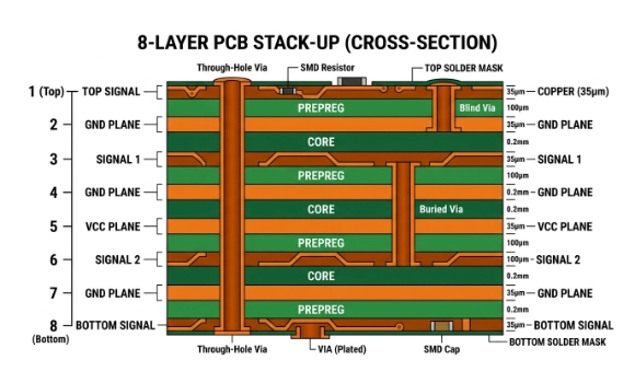
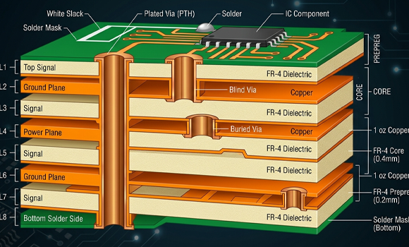
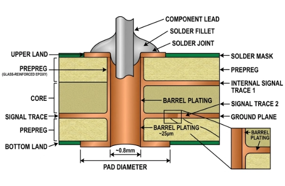
Via-in-Pad (VIP) is an advanced PCB design technique where a via is placed directly inside the pad of a surface-mounted component.
Unlike traditional “dog-bone” fanout routing, VIP eliminates the need for traces between pads and vias, enabling higher routing density and compact PCB layouts.
To ensure reliability, VIP structures are typically:
- Filled with epoxy (resin plugging)
- Planarized for a flat surface
- Capped with copper plating
This ensures proper soldering and prevents defects during assembly.
Why Use Via-in-Pad in PCB Design?
Via-in-Pad is widely used in HDI (High-Density Interconnect) PCB designs, especially for fine-pitch components.
Key Benefits:
1. Increased Routing Density
VIP allows designers to route signals directly beneath components, making it ideal for:
- BGA (Ball Grid Array)
- QFN packages
- Fine-pitch ICs (≤0.5 mm pitch)
2. Improved Signal Integrity
By shortening signal paths and reducing loop area, VIP helps:
- Minimize parasitic inductance
- Reduce signal reflection
- Improve high-speed performance
This is critical for high-frequency and high-speed PCB designs.
3. Enhanced Thermal Performance
Via-in-Pad also acts as a thermal pathway, transferring heat from components to internal copper planes.
- Reduces junction-to-ambient thermal resistance
- Improves heat dissipation efficiency
- Extends component lifespan
4. Space Optimization
VIP eliminates the need for fanout traces, allowing:
- Smaller PCB size
- Higher component density
- Reduced layer count (in some cases)
Via-in-Pad vs Traditional Fanout (Dog-Bone)
| Feature | Via-in-Pad (VIP) | Dog-Bone Fanout |
| Routing space | Maximum efficiency | Requires extra space |
| Signal path | Shorter | Longer |
| Thermal performance | Better | Moderate |
| Manufacturing complexity | High | Low |
| Cost | Higher | Lower |
VIP becomes essential when routing space is extremely limited or performance requirements are high.
Via-in-Pad Fabrication Process
VIP manufacturing is significantly more complex than standard vias.
Typical Process Flow:
- Drilling and plating (form via barrel)
- Resin filling (plugging)
- Curing process
- Planarization (critical step)
- Copper capping (plating over the via)
- Surface finishing (ENIG, etc.)
Each step must be tightly controlled to ensure flatness, conductivity, and reliability.
Why Filled and Capped Vias Are Mandatory
Using open vias in pads leads to serious assembly defects:
- Solder wicking → solder flows into the via
- Insufficient solder joints
- Solder leakage to opposite side
- Short circuits or weak connections
Industry best practice requires filled and capped vias (IPC-4761 Type VII) for all VIP applications.
Reliability Challenges of Via-in-Pad
Despite its advantages, VIP introduces several reliability risks:
1. Void Formation
Incomplete filling may trap air inside vias.
- Leads to outgassing during reflow
- Causes voids in solder joints
2. CTE Mismatch
Differences in thermal expansion between:
- Copper
- Resin fill
- PCB substrate
→ Can cause mechanical stress and long-term failure.
3. Planarity Issues
Poor planarization can result in:
- Uneven pad surface
- Poor solder joint quality
- Assembly defects
IPC Standards for Via-in-Pad
To ensure manufacturability and reliability, VIP must follow industry standards:
- IPC-4761 Type VII → filled and capped vias (required for VIP)
- IPC-2221 → general PCB design guidelines
- IPC-6012 → performance and qualification standards
These standards define:
- Filling requirements
- Annular ring tolerances
- Surface flatness criteria
Design Guidelines for Via-in-Pad
To achieve optimal results, follow these best practices:
- Use via filling + copper capping (mandatory)
- Ensure tight annular ring control
- Maintain flat surface (low dimple depth)
- Optimize via size vs pad size
- Work closely with PCB manufacturer for DFM
For ultra-high-speed designs, even small geometry variations can affect impedance and performance.
When Should You Use Via-in-Pad?
VIP is recommended when:
- BGA pitch ≤ 0.5 mm
- High-speed signals (>10 Gbps)
- High-power thermal requirements
- Space-constrained PCB layouts
It is not recommended for low-cost or simple designs due to higher fabrication cost.
Conclusion
Via-in-Pad (VIP) is a critical technology for modern high-density PCB design, enabling:
- Higher routing density
- Better signal integrity
- Improved thermal performance
However, these benefits come at the cost of increased manufacturing complexity and stricter process control.
For advanced electronics—especially HDI, high-speed, and compact devices—VIP is not just an option, but often a necessity.
Ready for Production? Kickstart Your Project Now. info@ysx-tech.com
Unsure About the Design? Consult with Our Lead Engineers Today. contact us
Share on Social:


