




PCB Gold Fingers: Definition, Types, Design & Applications

What Are PCB Gold Fingers?
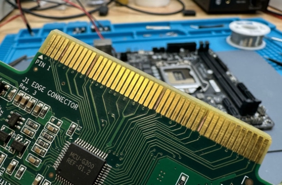
PCB gold fingers refer to the gold-plated contact pads located along the edge of a printed circuit board (PCB). These connectors act as the interface between a PCB and other electronic components, such as motherboards, expansion cards, or peripheral devices.
They are commonly used in applications like graphics cards, RAM modules, SSDs, and industrial control boards, where reliable signal transmission and repeated insertion are required.
Why Are Gold Fingers Used on PCBs?
Gold is chosen as the plating material due to its unique physical and electrical properties:
- Excellent conductivity – ensures stable signal transmission
- Corrosion resistance – prevents oxidation over time
- High durability – withstands repeated insertion and removal cycles
- Low contact resistance – improves overall connection reliability
Compared to other finishes, gold plating significantly enhances the lifespan and performance of PCB edge connectors.
Types of PCB Gold Finger Plating
1. Electroplated Hard Gold (Recommended)
- Contains gold alloyed with cobalt or nickel
- High hardness and wear resistance
- Ideal for frequent insertion applications (PCIe, RAM, GPU)
2. ENIG (Electroless Nickel Immersion Gold)
- Thinner and softer gold layer
- Lower cost and easier soldering
- Suitable for low-cycle or prototype applications
Hard gold plating is the industry standard for high-reliability connectors due to its superior durability.
Common Types of Gold Fingers
Depending on the design requirements, gold fingers can be categorized as:
- Standard (flush) gold fingers – uniform length and spacing
- Segmented gold fingers – partially separated contacts
- Long-short (staggered) gold fingers – varying lengths for sequential contact
These variations are used to improve insertion stability and functional sequencing in advanced electronic devices.
Key Applications of PCB Gold Fingers
Gold fingers are widely used in both consumer and industrial electronics:
- Computer hardware – RAM, GPUs, expansion cards
- Storage devices – SSDs (M.2 interfaces)
- Communication devices – routers, network cards
- Industrial equipment – control modules and embedded systems
They serve as critical interconnection points, enabling high-speed signal transmission between different PCBs.
PCB Gold Finger Design Guidelines
To ensure reliability and manufacturability, gold fingers must follow strict design rules:
- Keep plated through holes (PTH) away from gold fingers
- Maintain a clearance zone (≥1.0 mm) from other features
- Avoid solder mask or silkscreen coverage on contact areas
- Ensure smooth and clean plating surface
- Position gold fingers facing outward for proper insertion
Failure to follow these guidelines may lead to poor contact, signal loss, or mechanical damage.
Gold Finger Beveling (Chamfering)
To facilitate easy insertion into connectors, PCB edges with gold fingers are typically beveled:
- Angle: 30°–45°
- Purpose:
- Reduce insertion force
- Prevent connector damage
- Improve mating alignment
Beveling is a critical step in the PCB manufacturing process for edge connectors.
Gold Finger Plating Thickness
The thickness of gold plating directly impacts durability:
- Typical range: 2–50 microinches (µin)
- Standard applications: ~30 µin
- Higher thickness = better wear resistance but higher cost
Selecting the right thickness is essential for balancing performance and budget.
Conclusion
PCB gold fingers are essential components for high-reliability electrical connections in modern electronics. By combining excellent conductivity, durability, and corrosion resistance, they ensure stable signal transmission across a wide range of applications.
For high-performance PCBs, choosing the right plating type, thickness, and design specifications is crucial to achieving long-term reliability and optimal performance.
Ready for Production? Kickstart Your Project Now. info@ysx-tech.com
Unsure About the Design? Consult with Our Lead Engineers Today. contact us


