





PCB X-Ray Inspection: How AXI Detects Hidden Assembly Defects
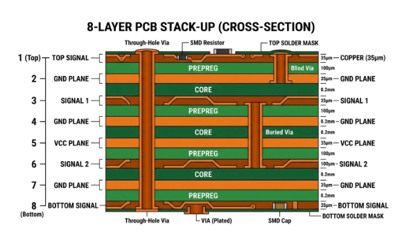
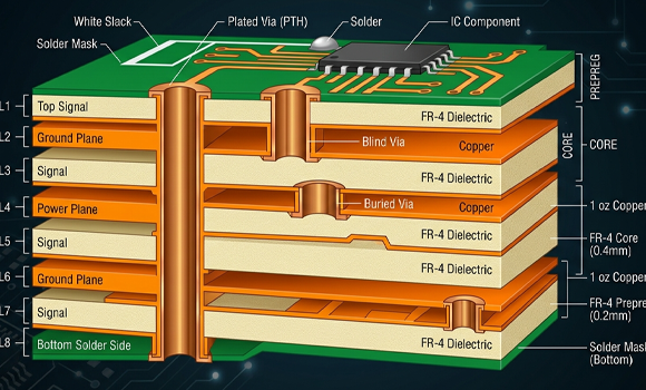
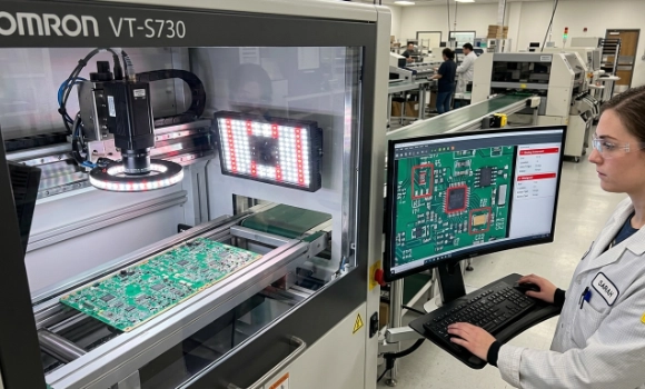

PCB X-ray inspection uses radiographic imaging to evaluate hidden solder joints in PCB assemblies without dismantling components. Automated X-ray inspection, or AXI, helps assess packages such as BGA, CSP and QFN, where optical access is limited. Images can reveal solder voids, bridges and other structural irregularities, depending on equipment capabilities and viewing angles. Inspection results should be assessed against applicable project criteria. AXI complements optical inspection and electrical testing, helping manufacturers investigate assembly defects before products move to subsequent verification.
Working Principle of AXI
AXI is based on the principle of differential X-ray absorption:
- Dense materials (solder, copper) absorb more radiation → appear darker
- Less dense materials (air voids, resin) absorb less → appear brighter
The system captures these differences to reconstruct internal structures.
Key imaging mechanisms:
- Transmission imaging (2D)
- Oblique angle imaging (2.5D)
- Computed tomography (3D CT reconstruction)
AXI System Architecture
A complete AXI system includes:
- X-ray source tube
- Detector (flat panel / image intensifier)
- Motion control stage
- Image processing software
- AI defect recognition module (advanced systems)
Manufacturing Defects Detected by AXI
AXI is specifically designed to detect hidden structural and solder-related defects, including:
Solder joint defects:
- Voids (gas entrapment inside solder)
- Head-in-pillow (BGA separation defect)
- Cold solder joints
- Insufficient wetting
Structural defects:
- BGA misalignment
- Bridging under components
- Internal layer voids in some stackups
Critical insight:
These defects are not visible under AOI or visual inspection, making AXI essential.
AXI vs AOI (Critical Comparison)
| Feature | AXI | AOI |
|---|---|---|
| Inspection Type | Internal (3D/2D) | Surface |
| Technology | X-ray imaging | Optical imaging |
| Hidden solder joints | Detectable | Not detectable |
| Speed | Slower | Faster |
| Cost | Higher | Lower |
| Application | High reliability PCBA | General SMT inspection |
👉 Industry rule: AOI + AXI = complete inspection coverage
AXI Inspection Methods
1. 2D AXI
- Fast imaging
- Used for production screening
- Limited depth interpretation
2. 2.5D AXI
- Tilted imaging improves defect visibility
- Common in SMT production lines
3. 3D CT AXI
- Full volumetric reconstruction
- Used for failure analysis and aerospace-level validation
AXI Process Flow in Manufacturing
- PCB assembly completed (SMT reflow)
- PCB enters inspection stage
- AXI scanning performed
- Image reconstruction
- Automated defect detection
- Engineer validation
- Quality report generation
Design for Inspection (DFI Considerations)
To ensure AXI effectiveness:
- BGA pad design must allow void visibility
- Avoid overlapping high-density copper shadows
- Ensure consistent solder volume
- Maintain proper component spacing for imaging clarity
IPC and Industry Standards
AXI is aligned with:
- IPC-A-610 (acceptability of electronic assemblies)
- IPC-7095 (BGA assembly guidelines)
- IPC-6012 (PCB performance standard)
For automotive and aerospace:
- ISO 26262 (functional safety)
- AS9100 (aerospace quality system)
Limitations of AXI
Despite its advantages:
- High equipment cost
- Slower than AOI
- Requires skilled interpretation in complex cases
- Shadow overlap in dense assemblies may affect clarity
Ready to implement X-ray inspection in your PCB assembly process?
Choosing the right inspection system is critical to ensuring product quality and yield. YSX provides expert guidance and tailored X-ray inspection solutions—ranging from streamlined 2D systems to advanced 3D CT technology—to meet your specific application needs.
Ready for Production? Kickstart Your Project Now. info@ysx-tech.com
Unsure About the Design? Consult with Our Lead Engineers Today. contact us
Share on Social:


